 |
|
Optics can be found virtually everywhere, from fiber optic couplings to machine vision imaging devices to cutting-edge biometric iris identification systems. Despite the many applications that depend on optics, most of our customers are not optical engineers. As a result, they require aid in specifying the correct optical components for the mechanical, electrical, and various other existing applications.
Even qualified engineers send us prints that are at either of two extremes: under-specified or over-specified. In either case, understanding the application is the key to satisfying the needs of the customer. This understanding allows us to offer our advice as to the correct choice of components, specifications and tolerances. These factors need to match the requirements of the application in question and need to justify the associated costs. Simply copying catalog specifications is not the best solution. This article will concentrate on the use of common optical specifications. |
|
 SURFACE ACCURACY SURFACE ACCURACY
After a design is successfully completed, we can determine the characteristics of each optical surface in the system and tolerance them according to manufacturing capabilities. This is done with an emphasis on the value and uniformity of the shape, as well as on the cosmetics of each surface. The maximum allowable deviation of an optical surface from a perfect surface is described by Surface Accuracy. There are several terms associated with accuracy, as follows: |
|
|
Surface Flatness?is the deviation for a plano surface such as a window or mirror. When a test plate (typically an optical flat) is held in contact with the work piece (the part under inspection), a contour map is visible as light and dark bands. These dark bands are called Newton's rings or fringes. Due to the air gap between the surfaces, each ring corresponds to the vertical distance between the test plate and the surface under inspection. Since the test plate in this case is a clear, flat reference, the air gap is very small so the surface flatness is defined in terms of wavelength (very small unit of measure); i.e. 1/4 wave or?l/4. The spacing between rings is equal to one-half the wavelength of the illumination source; i.e. 1/4 wave = 1/2 ring. A monochromatic green light at the 546.1 nm mercury line or helium-neon red laser line at 632.8 nm is used for illumination. Typically, only values less than 1/4 wave are considered to be precision and values less than ll/10 to be high precision.
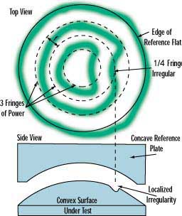
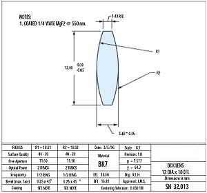
Power is used when dealing with a curved surface to define the deviation of the fabricated surface radius from the radius of an inversely shaped test plate. The test plate is a highly calibrated reference gauge (see Figure 1). This deviation is also referred to as surface fit; i.e. how well the work piece "fits" the test plate. The number of rings visible is used to identify the power of the surface. Again, each ring is equivalent to 1/2 of the test wavelength. The surface is checked using this procedure at several different stages of production. Note that even though our optical prints use power and irregularity to specify maximum allowable deviations (see Figure 2), radii tolerances are used for the fabrication of actual test plates.

(Figure 1)

(Figure 2)
Irregularity is used to define how the surface deviates from the perfect shape of the test plate, as demonstrated by a spherical or cylindrical surface. Thus, the uniformity of the rings' shape indicates the limit of the surface's regularity. This deviation is also known as surface figure. As a specification, it is important to note that in order to properly inspect irregularity, it cannot be much smaller than the power or else you will not be able to ensure the irregularity value. A typical rule of thumb is to use a maximum power of 4 or 5 times the irregularity. Most optic shops work the power out from a stated irregularity.
Please note that the overall focal length tolerances provided in our catalog are tested as final overall performance - they are not manufacturing tolerances, but determined from limitations set by the power and irregularity specifications.
|
|
An optical flat is a precisely polished flat surface, used as a reference against which the flatness of an unknown surface may be compared. ultiQuest Technology offers both single surface and dual surface optical flats in either Zerodur? or Fused Silica. We offer three different levels of accuracy for our single surface flats: 1/4 wave, 1/10 wave, and 1/20 wave. For our dual surface flats, 1/4 and 1/10 accuracies are available. |
 SURFACE QUALITY SURFACE QUALITY
This refers specifically to the cosmetic condition of an optical element's surface. During the grinding and polishing stages of fabrication, small defects can occur, such as scratches and digs. A scratch is any mark or tear and a dig is any pit or divot in the element's surface. The specification used for the maximum allowable flaws is denoted by a combination of numbers, the scratch number followed by the dig number; for example 60-40. The lower the number, the higher the level of quality. For example, a 60-40 value is common for research and industrial applications, whereas a 10-5 value represents a high quality standard for laser applications.
It is important to note that neither the scratch nor the dig numbers actually correspond to a specific number of defects. Instead, they reflect the quality of an optical surface as determined by a visual comparison to a precisely manufactured set of standards. This process is in accordance with the MIL Spec. Scratch and dig evaluation is as defined by the US Military Specification for the Inspection of Optical Components, MIL-O-13830A.
There is no direct correlation between scratch number and the actual size of a scratch on an optical element's surface. As a common reference, the scratch number relates to the "apparent" width size of an acceptable scratch. However, there is some ambiguity since it also includes the total length and number of allowable scratches. Dig numbers do relate to a specific size of dig. For example, a 40 dig number relates to a 400 μm (or 0.4mm) diameter pit. Coating quality is also held to the same Scratch-Dig specification as the surface of an optic.
Surface Quality inspection typically includes additional criteria, such as staining and edge chips. Overall cosmetic inspection also includes defects within the material, such as bubbles and inclusions, including striae. Imperfections of this nature can contribute to scattering in systems involving lasers and image defects (if at or near the image plane). Inspection of surface accuracy and quality is limited to the component's clear aperture. |
|
 CENTRATION CENTRATION
The mechanical axis and optical axis exactly coincide in a perfectly centered lens.
Optical and Mechanical Axes
For a simple lens, the optical axis is defined as a straight line that joins the centers of lens curvature. For a plano-convex or plano-concave lens, the optical axis is the line through the center of curvature and perpendicular to the plane surface.
The mechanical axis is determined by the way in which the lens will be mounted during use. There are typically two types of mounting configurations, edge mounting and surface mounting. With edge mounting, the mechanical axis is the centerline of the lens mechanical edge. Surface mounting uses one surface of the lens as the primary stability for lens tip and then encompasses the lens diameter for centering. The mechanical axis for this type of mounting is a line perpendicular to the mounting surface and centered on the entrapment diameter.
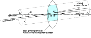
Ideally, the optical and mechanical axes coincide. The tolerance on centration is the allowable amount of radial separation of these two axes, measured at the focal point of the lens. The centration angle is equal to the inverse tangent of the allowable radial separation divided by the focal length.
Measuring Centration Error
Centration error is measured by rotating the lens on its mechanical axis and observing the orbit of the focal point. The centration error ( qc) is then given by

where rorbit is the radius of the focal orbit and f is the focal length of the lens.

Centration and Orbit of Apparent Focus
Doublets and Triplets
It is more difficult to achieve a given centration specification for a doublet than it is for a singlet because each element must be individually centered to a tighter specification, and the two optical axes must be carefully aligned during the cementing process. Centration is even more complex for triplets because three optical axes must be aligned. The centration error of doublets and triplets is measured in the same manner as that of simple lenses. One method used to obtain precise centration in compound lenses is to align the elements optically and edge the combination.
Cylindrical optics can be evaluated for centering error in a manner similar to simple lenses. The major difference is that cylindrical optics have mechanical and optical planes rather than axes. The mechanical plane is established by the expected mounting, which can be edge only or the surface-edge combination described above. The radial separation between the focal line and the established mechanical plane is the centering error and can be converted into an angular deviation in the same manner as for simple lenses. The centering error is measured by first noting the focal line displacement in one orientation, then rotating the lens 180 degrees and noting the new displacement. The centering error angle is the inverse tangent of the total separation divided by twice the focal length.
|
 EDGE TREATMENT EDGE TREATMENT
There are several terms associated with the treatment of edges. The most basic is a cut edge; this is literally what it means. A large sheet of glass is either "cut" using a scribe and break technique or cored for circular pieces. The edges are left as is which can leave sharp edges. The next edge type is swiped or seamed edges which means that all the sharp edges are removed. The final type is a ground edge which provides an even mounting surface and gives a uniform cosmetic appearance to the perimeter of the optic. The better the treatment of the edge, the less likely it may become chipped in handling. Edge chips are not permitted within the optics' stated clear aperture. Edge chips are typically defined for optical windows and first surface mirrors to have maximum values of 0.25 to 0.5mm.
Bevels are clean ground edges used to prevent edge chips or simply as protective chamfers. Our bevels are defined as maximum face widths at 45°, with a standard tolerance of ±15°. For micro optics, we do not bevel the edges (since the attempt will likely cause chips). Also, we do not bevel the edges for small radii meeting the diameter edge at large angles. If the diameter = (0.85 x radius of curvature), then no bevel is used. The actual clear aperture (CA) value used will typically be smaller than that defined by the bevels with a maximum possible CA calculated as follows:
 |
 PRISM ANGLE ACCURACY PRISM ANGLE ACCURACY
Typically, the relative angle between the reflecting surfaces (as in a roof) needs to have a critical tolerance in order to maintain a maximum allowable angular deviation. However, depending on placement in a system, the other angle(s) could be toleranced to limit aberration effects. Angle tolerances for prisms are inspected using an autocollimator with the prism oriented as a retro-reflector. This is only suitable for testing 90° and 45° angles; i.e. as in a right angle prism. Note that although this specification relates to the physical edge of two reflecting surfaces, it is typically tested as beam deviation. |
|
 THICKNESS THICKNESS
The importance of an element's axial thickness depends greatly on its role in a system and can vary dramatically. Thickness refers specifically to the center thickness of a lens or spacing between elements. For curved surfaces, a reasonable operating tolerance runs ±0.1mm. For flat surfaces, however, the production of large sheets of non-polished glass yields larger variances in thickness. Thickness will vary greatly depending on sheet size and where on the sheet the measurement is made. In order to accommodate this fact a nominal tolerance value is used meaning that no specific thickness tolerance is defined. Over time, nominal thickness tolerance has generally been accepted to be ±0.015" to 0.020". Again, this refers to glass that is not polished after fabrication.
If a specific thickness or precision surface accuracy is needed then polishing is clearly required and higher orders of tolerancing can be maintained. Typically, a 6:1 diameter to thickness ratio is used as a rule of thumb for high accuracy plano surfaces in order to prevent warping in fabrication or in the final mounting. Higher ratios may be used for lenses depending on radii and diameter values.
Edge thickness is used as a "reference" for lenses meaning that it is not a manufacturing limit. Edge thickness is actually a calculated value which depends on radii, diameter, and center thickness. It is thus used as a reference to indicate physical limitations for mounting considerations.
|
|
If you would like to see other topics covered or more detailed information, please contact our via e-mail at info@ultiquestcom.com |
|
| |
|
|
| |
Services |
 |
 Contact Contact
If you have any questions or comments, please contact us by filling-in the mail form.
|
|
|


